I cannot believe it has been almost a year since I started my journey into FPGA development on the MISTer. To be honest, I didn’t even think I would get this far and release a core for Battle Bakraid, Batrider and Garegga (https://github.com/MiSTer-devel/Arcade-Raizing_MiSTer), and I hope you have been following my progress reports on Twitter.
One of my stated goals at the start of this effort was to give back to the community and make educational resources available for more folks to get into core development. I made a lot of mistakes and spent a lot of time trying to figure out the right workflow that worked for me, and so through this series of posts I will take you through my ideal workflow that I have created for FPGA core development. So, I will dive right in here.
Starting Out
Before starting on any core, I strongly recommend actually looking at the board and actually doing some diagrams in KiCAD to construct a rough schematic. That is what I did after becoming lost in details. It only started to all come together once I looked at the components and how they interface with each other. So, I highly recommend that you obtain or find high resolution pictures of the board in question and start tracing things out. I don’t like damaging expensive boards, so I used a multimeter and traced out much of the connections. I did not construct a complete schematic, but only enough until I had an understanding of how things communicated with each other on the board.
Why is this important?
Well, you see the arcade boards are analog circuits that interact with each other. The goal is to take the analog circuits and make a digital circuit design out of them; the FPGA model. If you don’t have the board and are relying on software emulators to do this, you will run into problems almost immediately. The biggest among them is that most emulators have a framework established that abstracts the emulation into different layers, so you probably wont get the under the hood details you need to create a detailed design. Secondly, software emulation is different than FPGA. Yes, they are both emulation of different flavors, but when you create an FPGA based design, you have to relate that back to the analog circuit models of the original board. So, if you are following a software emulator, it’s going to be hard to adapt that design directly to a circuit model that is continuous.
Software emulation is synchronous. The goal is to render frames at the end of the day per second. You can run billions of lines, block the CPU and other processes and take your sweet time to render that frame and push it. With FPGA, things work on strict timings and is fully async (and yes, by the way, I am well aware the meaning of “async” and “sync” are different in an FPGA context, but I am talking about the software program context here). The rendering subsystem and audio parts continuously run while the CPU program is running. There’s no waiting, unless you somehow halt the cpu or delay it while you do things, but that’s not really how it works from a practical perspective. Things must be done on time every time to be a good design.
So, software emulation is a different beast entirely than an FPGA design. You can use current emulators out there to fill gaps in your understanding, but I highly recommend that you do not base your FPGA design on it. It is not a good idea at all, and is going to waste a lot of time.
Creating a Usable Diagram
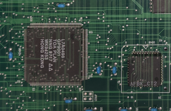
Get access to the board. If you own boards already, it’s a good idea to start with those for practice. Take a high resolution scan or photo of both sides of the board. Just fill the frame as much as you possibly can and try to get an even lighting.
Take these 2 pictures, and stack them in an image editing program like gimp and change the opacity of the top to see through to the bottom layer. You should end up with something like this (one section as an example):
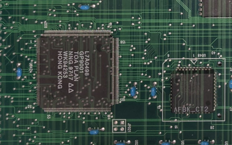
Now, what this lets you do is aid in a good physical inspection of the board. You can see the top level (parts side) components and also the solder side traces. The top parts side components all connect to each other somehow and interact, so having the solder side as a continuous see-through will help you figure out how quickly and follow lines.
Get a multimeter as well. You will use that to see which lines on which components connect to which pins on other components and confirm. This is a tedious process, but unless you want to take your HAKKO and desolder all the components and risk destroying your board, this is the best way.
Next, open KiCAD and start diagramming. I did this process for a few weeks until I had a good understanding of the board. I ended up with the partial schematic below:
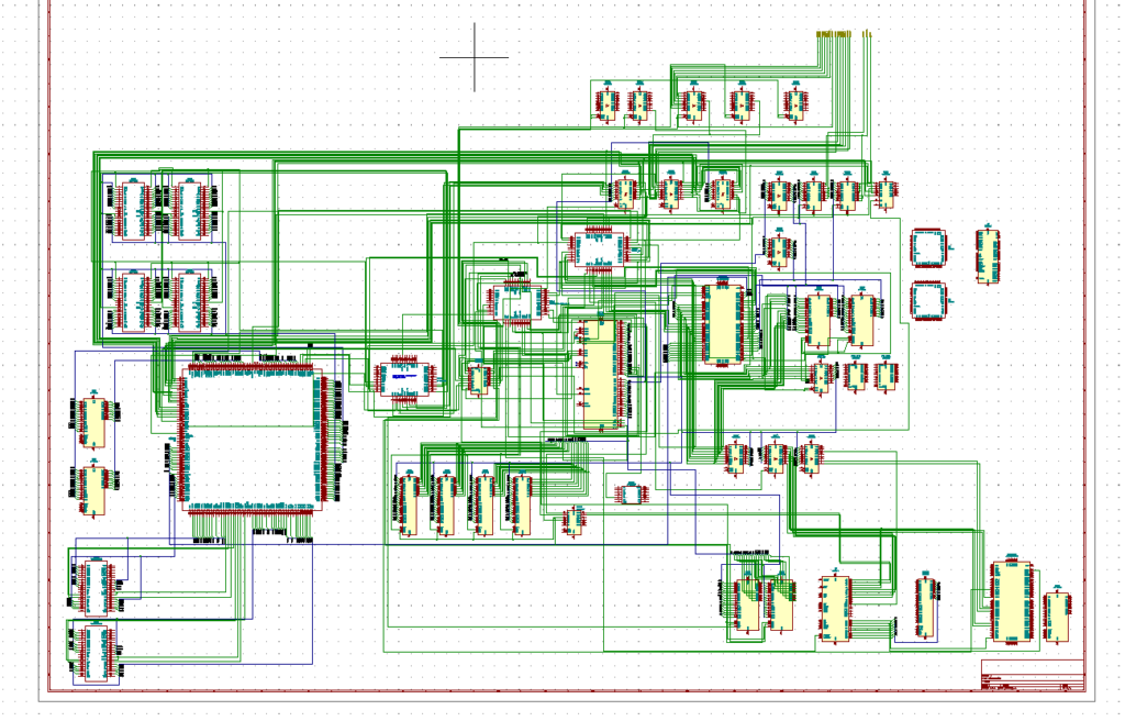
At the end of this process, I had a very good understanding of how the parts side components interacted with each other, what pins drove logic, etc. From here, you should now create a high level block diagram of the system.
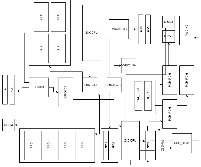
The above diagram I did just now is a highly simplified version, but not very far off from what you should produce. What this should tell you at the end of the day is how the different components communicate with each other on the board. This is going to be a roadmap for your FPGA implementation. There are details you will figure out along the way, like what do the custom chips do, how does RAM work, address bus, etc.
You should study your diagram very carefully and try to ask yourself questions about how something works, or communicates with another component. You can use current emulator sources to fill in your gaps in understanding.
Inventory
Now, once you have all your diagrams and block diagrams constructed, the next thing you have to take a look at is how to make the FPGA design. The block diagram you should have created is a roadmap to how you might implement the design in FPGA.
To do this, you have to now figure out if you have existing IP (ie. pre-built verilog modules) to fill out and implement your design, or if you have to go creating new things to make it work.
From the above block diagram, I know that I would have to create new IP or modules for the GP9001, the custom chips and the interaction components between the parts. However, the 68k CPU and Z80 already exist out there, so I can use that. the JT51 module is good for the ym2149, and then the JT6295 should cover the OKI chips. I have to create modules for the GALs on the board as well.
At the end of this process, you should have an inventory of what exists and what doesn’t, and start things from there.
What’s Next?
In the next part of the series, I will go over how to start the coding and design process in verilog and the order of implementation. As I go through the implementation, I will also describe the design of the system in detail as I work through one by one.
– pram0d