In the last part, we talked about putting together a loader which ensures that the game rom data is made available to the MiSTer and FPGA for use in SDRAM. Today, I will show you how I put together a basic CPU module, which is the heart of the overall system. A lot of this will be biased toward using a 68k CPU, which is fairly common in a lot of 90’s games, but the same steps can also apply whether you are using a Z80 or other CPUs which are specific to your game.
What the CPU Module Should Do
The CPU module, should contain logic that is specific to the workings of the target CPU and address bus. It should contain outbound connections to other modules which the CPU is directly interfacing with, which potentially could be sound or graphics processing units, in addition to rom and external memory. Inbound, should be any other potential settings that are passed to the CPU and read such as inputs, dip switches or miscellaneous I/O.
How to Start a CPU Module
First, take a look at the technical specifications for the game you are trying to put together, and find out what the main CPU is. Some games have multiple CPUs, one for the game program and sound program driver, for example. Other games might even have multiple CPUs for the game itself handled through multiple program ROMs. Whatever the main CPU is though, you should have a corresponding program rom in your romset you are working with.
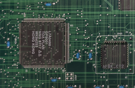
So, in the case of Battle Garegga, the prg0 and prg1 roms in the romset are for the 68k program. The roms contain the even and odd bytes for the program rom, respectively, and should be interleaved in the loader process prior to passing the data to the CPU. Be very careful when doing this, and take a look at the data closely. Sometimes, the way its dumped is byteswapped the other way compared to what it actually was on the original chips. Sometimes it’s in a different endian order.
One surefire way to tell is to construct your MRA, as we did in the last post of the series, and then use the tool mra-tools (https://github.com/sebdel/mra-tools-c). Using this tool, you should be able to pass the directory where your romsets are located, as well as an MRA and get out a contiguous .rom file. This .rom file, is exactly what the MiSTer should produce at the end of the “assembling” process, and if you take a look at that data in the hex editor, you should be able to see if your data is being passed correctly or not to your game:

Above, are some string data as a result of the interleaving and assembling. A sure sign it is correct is if string data appears in the proper order and not jumbled or backwards. All 3 of Yagawa’s games have his signature, as a fun fact, in the game program rom header section:


In any case, as you can imagine, the first step to creating the CPU module is to ensure that your program rom data is correct, and secondly, that it is accessible properly from the CPU module. Next, you will have to figure out what your target CPU is, where the verilog module you are using is located, and how to interface with it. This process requires some knowledge of the target CPU’s workings, so don’t be afraid to google information on the target CPU and how it works, and how to hook it up pin wise.
Hooking up the CPU
First, you will need to instantiate the CPU module. Again, this post will be biased towards a 68k, as that is what Garegga uses, but the process is not so different for others:
fx68k u_011 (
    .clk        (CLK96),
    .extReset   (RESET96),
    .pwrUp      (RESET96),
    .enPhi1     (CEN16),
    .enPhi2     (CEN16B),

    // Buses
    .eab        (A),
    .iEdb       (cpu_din),
    .oEdb       (cpu_dout),

    .eRWn       (RW),
    .LDSn       (LDSn),
    .UDSn       (UDSn),
    .ASn        (ASn),
    .VPAn       (VPAn),
    .FC0        (FC0),
    .FC1        (FC1),
    .FC2        (FC2),

    .BERRn      (1'b1),

    .HALTn      (DIP_PAUSE),
    .BRn        (BRn),
    .BGACKn     (BGACKn),
    .BGn        (BGn),

    .DTACKn     (DTACKn),
    .IPL0n      (1'b1),
    .IPL1n      (1'b1),
    .IPL2n      (int1),

    // Unused
    .oRESETn    (),
    .oHALTEDn   (),
    .VMAn       (),
    .E          ()
);
For the 68k, there are clocks and a shifted clock you must provide to the CPU in the first few pins, as you can see, as well as a reset signal.
Next, there are address bus pins. The 68k has a 24 bit address bus A[23:1]+UDS/LDS(A[0]). It produces addresses in accordance with a 16 bit addressing scheme (A[23:1]). According to the workings of the CPU, a valid address will appear on the bus when AS is low and BGACK is high. When this condition is met, your code should process the current address on the bus accordingly and do the thing you have to do with the data outputs or inputs (iE, oE). The thing you have to do, depends on eRW, read or write.
I wont go into the nuances or details of the other pins, as those are highly 68k specific and may not apply to you. For example, there’s a whole section and logic on how to generate the DTACK signal which tells the 68k that data is ready, or using the function counter FC pins for interrupt clearing etc. However, one other thing you should pay attention to is how interrupts are generated and used in the game program (IPL0-2).
For the Raizing games, there is only 1 interrupt that really matters, and that is an interrupt that is triggered on vblank start. If this interrupt is not correct, the game will not work. It will black screen. And, the pin it is on, is different for some games, so its not always the same pin. The 68K has 3 interrupt pins for a total of 7 interrupt levels. You should be able to deduce how the interrupts are working by looking at current emulators to see if you have it correct, or by looking at those pins on the real board and tracing them back to other components to see how they are driven.
Constructing the Address Bus
Once you have the pinout for your CPU all hooked up, the next thing to do is figure out what your address and memory map look like for your target game. You can get the map from current emulators or websites out there.
For Battle Garegga, there’s this website (http://www.arcaderestoration.com/memorymap/629/Battle+Garegga+-+Type+2.aspx) that has a memory map of the game. The game has 2 CPUs, a Z80 and a 68K, which are both listed. This is the 68K one:
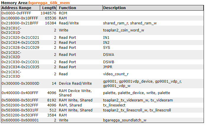
So, how do we use this information? Simple. When the address on the bus matches the designated values, we do that designated thing. Here is an example:
- These are 8 bit addresses, so you must add the UDS/ LDS to A[23:1]. For example, {A[23:1], !LDSn && UDSn}. If LDS is low and UDS is high, it means its an odd address (ie. an operation affecting the lower 8 bits only of the target), else it is even. However, if UDS is low, and LDS is high, it means it affects only the upper 8 bits. If both are low, that means its both, and the address is even. Since the 68k produces addresses in accordance with a 16 bit addressing scheme, the effective address could write to the lower 8bits, or the upper 8 bits by way of the UDS/LDS strobe, or both. So, the game could be doing both 8 and 16 bit operations via this method.
- Being that is the case, to make matters simple, what I do is I create an addr_8 wire. The addr_8 wire is basically {A[23:1], 0}. Then, in my address bus code, I process things depending on if the operation is read/write and the LDS/UDS strobes.
- Take ROM for example. ROM is designated by address 0x0 to 0xFFFFF. This means ROM is 0x100000 bytes long.
- When addr_8 is greater than or equal to 0, and less than or equal to 0xFFFFF, then we should send this request to SDRAM so that the location of the ROM program is given to the CPU on pins iE, which is 16 bits.
- The game program rom reads 16 bits at a time, so we can shift addr_8>>1 and pass this address directly to the SDRAM controller, which will in turn return to us the proper data for the address.
Another example is with RAM. As I mentioned, operations can affect 16 bits or 8 bits via the strobes. So, for RAM, that means you must segment your RAM into even and odd chips (as is on the real board) and use 16 bit addressing. I believe I explained this interleaving in the previous posts.
- RAM is designated by 0x100000 to 0x10FFFF. So, this RAM segment is 0x10000 bytes long.
- If the addr_8 is in this range, take addr_8>>1, and…
- If UDS is low, write to the first dpram for the high portion, if LDS is low, write to the low portion.
- As a result, writes can affect the even or odd bytes designated by the 16 bit address:
//CPU WRAM 0x100000-0x10FFFF
jtframe_dual_ram16 #(.aw(15)) u_cpu_wram(
    .clk0(CLK96),
    .clk1(CLK96),
    // Port 0 writes & reads from 68k
    .data0(wram_cpu_data),
    .addr0(A[15:1]),
    .we0({sel_ram && !RW && !UDSn, sel_ram && !RW && !LDSn}),
    .q0(),
    // Port 1
    .data1(),
    .addr1(A[15:1]),
    .we1(2'b00),
    .q1(main_ram_q0)
);
The address bus implementation might entail other things, such as setting a reg, sending data to external modules, or other actions. But, the logic is the same. You take a look at the address value on the bus currently, and take the desired action.
Testing
Getting the address bus implementation right in the CPU module, as well as the corresponding interrupt and timing logic should result in the game booting up successfully from a program standpoint. Although, of course you wont see anything on screen because you have not done the graphics portion of the implementation which involves bitmapped fonts and such, but you should be able to see it booting.
So, how do we know exactly that our program rom and address bus is even working? For this critical task, I highly recommend creating a test bench. Personally, I use modelsim for all my test bench work. However, I understand you may not have access to this tool, and I have seen folks use verilator or iverilog, but I have not been able to use those tools successfully, so I don’t use them.
But, here is the general strategy I use to see whether the game is booting properly or not and performing the right POST sequential steps:
- Get access to the source code of a current emulator. I personally use Final Burn Neo, as I can open that in visual studio 2019 and make changes and introduce new debugging code to see how the implementation is working. One other reason I like FBN as opposed to MAME from a source perspective is that the emulator is not as abstracted as MAME and easier to follow from an implementation perspective. You might be able to use MAME, but I don’t have that setup on my machine currently, just the binaries.
- So, in Final Burn Neo, what I do is I add debug print statements on both the 68k address bus portion and also in the main game driver.
- In my CPU module, I also add a print statement to get the same information:
if(!ASn && BGACKn) begin
            //debugging
             if(debug)
                $fwrite(fd, "time: %t, addr: %h, uds: %h, lds: %h, rw: %h, cpu_dout: %h, cpu_din: %h, sel_status: %b\n", $time/1000, addr_8, UDSn, LDSn, RW, cpu_dout, cpu_din, {sel_rom, sel_ram, sel_sram, sel_z80, sel_gp9001, sel_io});
With this method, the $fwrite will write out to a file I have defined some lines above. I can compare the log output from the test bench to the one produced by the emulator which is known working, and iron out any issues in the booting process. This technique for address bus debugging is a very important thing to use especially for problematic games that don’t seem to boot for you. Basically, you will check if the address bus sequence matches that of the emulator, and if not, you can make changes until it does.
Next Steps
Now that you have your main CPU module constructed, as well as placeholder connections for external modules, the next step is to implement and design the subsystems of the game. These are systems like Audio and Graphics processing, as well as rendering.