Creating a CPU can be a very daunting task for someone. There’s a lot of functionality embedded all in a single chip, and not to mention the pinout and interfaces that chip has with other components on the board, as well as the timing.
I think after creating the TMS34010 CPU in Verilog myself, and it being the first time ever creating a CPU IP, there were a lot of things I was confused about. I ended up re-designing the CPU several times to fit within constraints and logical bounds of the FPGA platform as well. Although the CPU is working now in a well enough state functionality wise, I think perhaps there is room for improvement and efficiency, but that is a topic for another day. The first step is always to get something working, then you work on refinements and getting it to work “pretty”.
This article breaks down a workflow that I think is good to follow when creating a CPU IP Core, as well as introduces terminology that can be confusing to someone tackling this for the first time. I call my approach “the data approach” to creating a CPU, as I believe in treating the CPU as a black box with inputs and outputs, and verifying the data outcomes as a means for verification of the CPU Core. I don’t concern myself with timing (although timing information is also data that exists as an outcome), but I do tackle that after things are working logically. The approach described is geared of course towards the TMS34010 CPU as an example, but the same approach can be applied to any CPU you are designing.
What is a CPU?
A CPU is defined simply as “Central Processing Unit”. What it is supposed to function as in a system is to run processing logic and output results somewhere. The CPU communicates on a bus with other components in the system, and places the results either on its own internal storage registers, or it can place them in memory somewhere if it has a built in memory controller (as the TMS34010 does).
Additionally, the TMS34010 has GPU functions (ie. drawing pixels) and video output. However, these are simply other instructions that perform processing logic similar to the most basic instructions like add or subtract (though on a larger and more complicated scale), and places results in the VRAM connected to the CPU. So, overall, the CPU is just a black box that does stuff and places results in places.
Terminology
There are certain things and concepts you have to be aware of when you are looking into a CPU. A list below are important terms that you will come across, and what the meaning of them is.
- Register(s)/ CPU Register(s) – The most basic fundamental storage unit internal to the CPU. As it does stuff, temporary storage space is needed. The storage space persists until it is cleared by another instruction or operation usually. The TMS34010 has 2 register files that have 15 registers each of 32 bit. There are also GSP registers (which are also addressable outside the CPU, and usually hold information concerning video output or graphics functions). These are 16 bits in length.
- ALU – Arithmetic Logical Unit. The ALU is a central place where mathematical computations occur in the CPU. So, if an instruction needs to do adding or subtracting, for example, it will send the data to the ALU, and the ALU will perform the computation and return the results back, usually in an internal register. The TMS CPU also has support for rotations and logical bitshifting in the ALU as well as division and multiplication.
- Master Clock/ Local Clock – The CPU runs at a defined speed according to the clock that is passed to it. That is the Master Clock. However, the instruction timings and other workings in the CPU run at what is called a Local Clock. This is a clock that is derived from the Master Clock that exists external to the CPU, and in the case of the TMS, is 1/8th of that clock. This means that instructions are timed according to 1/8th of the clock speed of the master clock, for N cycles. For example, if Adding takes 1 cycle, they mean 1 clock cycle of the slower, 1/8th clock.
- Machine State/ Machine Cycle – The number of cycles of the Local Clock, not the Master Clock.
- Interrupt Routine/ Service Routine – An address in program rom that gets jumped to when an “interrupt” occurs. An interrupt is an event that triggers a jump (sometimes immediately, or immediately thereafter following the current instruction) to a specific location in the program rom. Once an interrupt is triggered, usually the processor state and registers are backed up to external “scratch” ram, and restored when the routine completes.
- State – Bit Flags that define the current state of the processor. The state of the processor carries over into subsequent instructions, and is used for logic in the program that is executing. It also holds information that is used for other processing in the CPU logic.
- External Interrupt – An interrupt trigger that comes outside of the CPU. Usually for a custom chip that sits alongside the CPU used for processing, or sound and/or video components. When these pins are triggered high or low, the CPU goes through the interrupt processing cycle and jumps to a predefined address in rom that contains the entrypoint to that routine to be executed.
- Entrypoint – The starting address for execution either of a routine or program. When the CPU starts, there is a predefined address that the CPU looks at which contains the address of the entrypoint, ie. where the program is supposed to start executing from.
- Opcode – A code that defines a particular instruction. Opcodes are gotten from the program rom, and then the corresponding codes are matched to an instruction. Each instruction has a different format, and can also be composed of multiple words as well.
- Microcontrol – A metaprogramming method. You can write a subset of functions, and then write external “microcode” to chain them together to do things of varying complexity rather than just writing direct code to do that specific thing. I use microcode in the TMS CPU because implementing everything in full Verilog took too many LE resources, so I created my own Microcode language and assembler (in Python) that I use to do all the instructions. However, I elected not to do this for the GPU as it is not important for games, its mainly used for POST screens, not the actual gameplay. I may refactor this in the future to save more LE. I estimate I can save around 6 or 7%.
Internal Architecture
Once you have the base information about the CPU, you should move to create an internal architecture. The internal architecture defines the main guts of the CPU and other modules contained within it. My suggestion on this is that you place all the main guts in a single file, at least to start. If you start out with too many modules, what is going to end up happening is it will be hard to manage and mold into the final architecture once you learn more about the CPU. Plus, depending on the CPU you are working with, a lot of the components may be shared, so it will be difficult with too many modules passing signals back and forth and then some need gating controls, which increases the complexity and consumes a lot of time on your end to make things work.
In my TMS CPU, there are some other side modules I have reserved for interfaces, however, most of it is in the main file. I have composed a rough diagram below on my internal architecture and how that looks like:
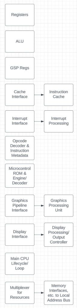
All the boxes in the middle existed in one file, and in refactoring, I have put many of them in submodules once everything was working properly. All the side boxes are separate modules that exist already at the outset; “controller” logic. There are submodules within the modules, but I left them out here for complexity. But, most stuff is central in one file, and there are lots of shared components in there.
Verification
Once you have something down that is workable, the next thing you want to do is see if the CPU you created actually runs code. To do this, I create a test bench that has the ROM in a giant block (byteswapped or not), and then hook that up to the local address bus, which in turn the CPU communicates on and retrieves data.
As such, the testbench you create needs to output data in a delimited file that you can use to verify the results in your favorite tool. I recommend using Excel, or, if you like scripting or have large data, you can use Python or another scripting language to iterate through results and do checks. The format I output looks like the following:
a0a0:00000830:ffc14900:010ffe70::01a80000:ffff0000:000201ff:01fe0000:02000000:0000800c:0000fbfb:ffd86a50:ffd9ad00:01400000:00000008:00126400:0101f120:0101eb80:ffffe000:00000000:00001000:008c01a4:00001000:00000000:fff7afa0:fbfb0000:000f000c:00000000:02038400:00000000:00008008:01a800a0:00000000:00000000::001c:003d:013d:0150:0003:001b:01ab:01b0:f010:fffc:01ab:0000:0000:0000:0000:0000:0000:0400:0002:0013:0013:0008:0000:0000:0000:0000:0000:0000:0200:0126:ef4c:0000:: 5: 5: 31:292704.0 ns
The format above is:
- opcode
- state
- program counter
- stack pointer
- reg A0-A14
- reg B0-B14
- GSP regs
- Local clock cycles taken
- Local clock cycles expected
- internal instruction ID (I use to match metadata, etc.)
- total sim time thus far
Similarly, I output the same thing on a current working implementation (ie. emulator such as FBNeo).
When doing this, I can verify that the 2 outputs are the same, and also use this data to track down issues. There are of course instances where the output of my thing is legit (after thorough investigation and confirmation), yet the one in the working known implementation is not. In these cases, I refer to the manual from the manufacturer and read carefully for arbitration between the two results. I have found many bugs in the current implementation this way, though minor, they affect the output of the game and how effects are produced and rendered on screen.
Optimization
Once everything is basically working, you will enter the optimization phase. The optimization phase entails looking at the columns for the local clock cycles taken and expected closely, as well as simplifying logic to cut down on unnecessary things. Doing this will speed up and streamline the execution and overall make for a more close implementation of the original CPU in FPGA.
These are some things you can consider in optimization:
- Cut down on registers, and put blocks of data storage elements in BRAM. Although it may technically be “slower”, this approach can cut down on LEs greatly and balance BRAM usage.
- Increase use of controller logic for shared resources. Instead of putting free regs all over the place, consider making a module a controller module and then having that broker access to data storage elements or other sequential logic. I do this, for example, for registers and memory access as well as the graphics pipeline and other side elements.
- Use microcode more efficiently. Create new types of instructions in the microcode that will help you consolidate and make execution simpler to follow. Doing this will reduce the number of clock cycles the instruction takes to execute all the steps, and make for a simpler design.
- It is OK to add ports and things that were not in the pinout of the original CPU for optimization. You don’t have to be a purist. The original CPUs were all analog, and here you are creating digital logic, so it isn’t going to be 1:1, and neither are the design principles. For example, I add extra ports for video and palette ram access as video is handled by the CPU internally. I also add a separate port for program rom access (64bit) because the original design of the CPU calls for the CPU internally accessing the program rom via it’s cache, not directly. Doing it through the main 16bit data bus would be horribly slow.
Next Steps
Next time, I will go over specific design patterns that I use to create the CPU and logic. This will include how to share access via priority encoders and other simple methods, as well as how to create controller logic and hook that in. Thereafter, I will have some discussion on the microcode engine, and how you can design something like that.